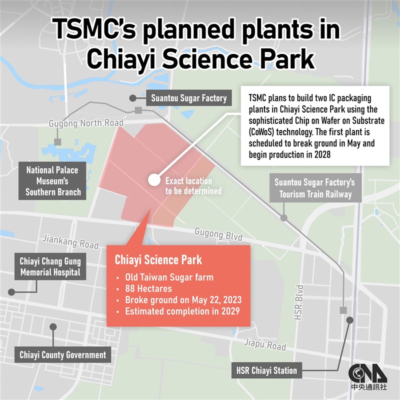
Taipei, March 19 (CNA) Contract chipmaker Taiwan Semiconductor Manufacturing Co. (TSMC) is set to build two packaging plants using the sophisticated Chip on Wafer on Substrate (CoWoS) technology at the Chiayi Science Park in southern Taiwan, with construction of the first plant scheduled to begin in May and mass production in 2028.
Here is a series of questions and answers (Q&A) about the planned advanced semiconductor packaging plants.
What is advanced packaging? What are the technologies for advanced packaging?
The techniques to fabricate silicon wafers have become more and more complicated due to the accelerating integration of chip processors with a diversity of functions, memory and key components, and an increasing demand for smaller chips and higher functionality.
In this context, chiplet technology emerged amid the industry's efforts to break the physical limitation of semiconductor manufacturing.
During the process of shrinking chip sizes, advanced packaging technologies played a crucial role, by raising calculation speeds, lowering power consumption and accelerating transmission speeds.
Advanced packaging technologies cover "fan-out/fan-in" packing, embedded die (ED), flip-chip assembly, and 2.5D/3D stacked die packages.
In response to strong market demand for three-dimensional integrated circuits (3DIC), TSMC introduced its advanced packaging 3D fabric platform, which includes front-end and back-end technologies.
The front-end process includes the SoIC (System on Integrated Chips) technology, which collocates with CoWoS and InFO (Integrated Fan-Out) in the back-end process. These offer benefits such as faster time-to-market, improved performance and efficiency, smaller form factors, and cost savings.
TSMC successfully integrates 3D chips manufacturing with the packaging process.

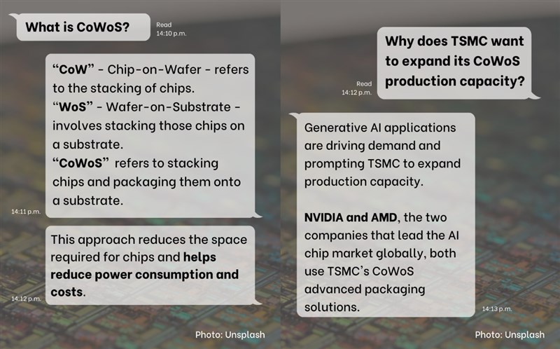
What is CoWoS?
CoWoS is a 3D packaging technology launched by TSMC that enables the integration of multiple dies and memory cubes into a single package.
The initial stage of chip stacking in CoWoS packaging, known as Chip on Wafer (CoW), primarily involves manufacturing at the fab using a 65-nanometer process. Following this, through-silicon via (TSV) is carried out, and the finalized products are stacked and packaged onto the substrate, known as Wafer on Substrate (WoS).
Why does TSMC want to expand its CoWoS production capacity?
Generative artificial intelligence (AI) applications are driving demand for high-end AI servers and the AI chips that are key for AI server processors, NVIDIA and AMD, the two companies that lead the AI chip market globally, both use TSMC's CoWoS advanced packaging solutions.
This has increased demand for TSMC's CoWoS production lines and prompted TSMC to actively expand production capacity.
What is TSMC's plan to expand CoWoS production capacity in the future?
Due to the robust demand for advanced packaging for AI chips, the shortage of TSMC's CoWoS capacity is expected to last until 2025. The company plans to double CoWos output this year with further expansion slated for 2025, TSMC CEO C.C. Wei (魏哲家) said in January.
TSMC has been investing in advanced packaging technologies for more than 10 years, including CoWoS, 3DIC and SoIC and expects to achieve more than 50 percent compound annual growth rate in production capacity.
It also continues to develop next-generation CoWoS advanced packaging techniques.
Which Taiwanese companies have also invested in the development of CoWoS?
Amkor has reportedly provided CoWoS solutions to Nvidia since the fourth quarter of last year. SPIL, a subsidiary of ASE Technology Holding Co., has also begun supplying CoWoS services since the first quarter of this year, according to industry insiders.
Powertech and King Yuan Electronics are also involved in advanced packaging of semiconductor products, industry insiders said.
What is the current situation in the global advanced packaging market?
Integrated device manufacturers (IDM), such as TSMC, Intel of the United States, and Samsung of South Korea, as well as semiconductor back-end professional outsourced semiconductor assembly and test (OSAT) service providers ASE, Amkor and China's JCET Group, are engaged in 2.5D packaging, with these six companies accounting for 80 percent of the world's advanced packaging wafer production capacity.
In addition, Japan's Sony, Taiwan's Powertech, the U.S.' Texas Instruments (TI), South Korea's SK Hynix (SK Hynix), and United Microelectronics Corp. (UMC) have also ventured into advanced semiconductor packaging.
What is TSMC's future monthly CoWoS production capacity plan?
From July 2023 to the end of last year, TSMC steadily expanded its CoWoS advanced packaging production capacity. As of last December, TSMC's CoWoS monthly production capacity increased to 14,000-15,000 pieces, and is expected to reach 33,000-35,000 pieces in the fourth quarter of this year, according to industry insiders.
![Four things to know about Bongkrekic acid]() Four things to know about Bongkrekic acidAfter a recent deadly food poisoning outbreak at the Xinyi branch of Malaysian restaurant chain Polam Kopitiam in Taipei caused two deaths, Bongkrekic acid was found in a blood sample taken from one of the deceased Thursday, forensic autopsy results showed.03/28/2024 11:27 PM
Four things to know about Bongkrekic acidAfter a recent deadly food poisoning outbreak at the Xinyi branch of Malaysian restaurant chain Polam Kopitiam in Taipei caused two deaths, Bongkrekic acid was found in a blood sample taken from one of the deceased Thursday, forensic autopsy results showed.03/28/2024 11:27 PM![Taiwan's tainted chili powder problem in detail]() Taiwan's tainted chili powder problem in detailTaiwan is facing a food safety problem involving the presence of "Sudan dyes" -- red synthetic chemical dyes banned in Taiwan for use in foodstuffs -- in chili powder imported from China. CNA has compiled answers to some frequently asked questions about the issue.03/11/2024 08:31 PM
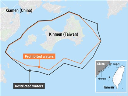
Taiwan's tainted chili powder problem in detailTaiwan is facing a food safety problem involving the presence of "Sudan dyes" -- red synthetic chemical dyes banned in Taiwan for use in foodstuffs -- in chili powder imported from China. CNA has compiled answers to some frequently asked questions about the issue.03/11/2024 08:31 PM![Taiwan and China's dispute over the waters around Kinmen]() Taiwan and China's dispute over the waters around KinmenOn Feb. 14, Taiwan's Coast Guard responded after a Chinese speedboat trespassed within 1.1 nautical miles of the eastern coast of the Island of Kinmen, setting off a chase in which the Chinese boat capsized, causing the deaths of two of the four men on board.02/19/2024 02:15 PM
Taiwan and China's dispute over the waters around KinmenOn Feb. 14, Taiwan's Coast Guard responded after a Chinese speedboat trespassed within 1.1 nautical miles of the eastern coast of the Island of Kinmen, setting off a chase in which the Chinese boat capsized, causing the deaths of two of the four men on board.02/19/2024 02:15 PM
- Cross-Strait
KMT caucus whip meets with senior Chinese officials in Beijing
04/27/2024 09:54 PM - Society
Hundreds of protesters in Taipei call for better child protection
04/27/2024 09:18 PM - Society
- Culture
Taiwan XR film wins first prize at Paris NewImages Festival
04/27/2024 07:20 PM - Cross-Strait
12 PLA planes cross Taiwan Strait median line: Defense ministry
04/27/2024 05:17 PM